Subgrid Particle Surface Film
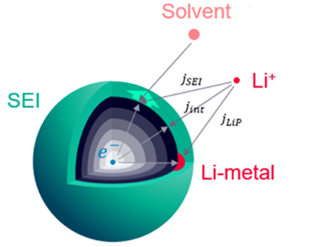
In batteries, parasitic side reactions can occur alongside the lithium intercalation process, such as the formation of the solid electrolyte interphase (SEI) or lithium plating (LiP). In Simcenter STAR-CCM+, the deposition of solid film on the surface of particles due to parasitic reactions is modeled by the Subgrid Particle Surface Film model.
The image below is an example of both the primary intercalation reactions and the parasitic side reactions occurring at the surface of the particle. As the SEI (green) layer thickens, lithium consumption reduces its cycling availability and the cell capacity. Additionally, the internal resistance of the battery increases. Lithium plating (red) is the deposition of metallic lithium on the surface of particles. Although, this does not form closed films around particles, the film is modeled as averaged over the particle.

The Particle Surface Film model assumes that the film that grows on the spherical particle is thin, which allows its volume to be approximated as:
- is the film thickness.
- is the surface area of the spherical intercalation particles.
The solid film thickness at time is calculated as:
- is the radius at the surface.
- is non-unity porosity.
- is the available volume fraction of the electrode porous phase (particle).
- is the solid volume fraction of the film porous phase. The solid volume fraction is used to calculate the initial film thickness and remains constant as the film thickness develops due to electrochemical reactions.
The growth of the film thickness is calculated as:
- is the molecular weight of the film material.
- is the density of the film.
- is the bulk substance electrochemical reaction flux of the film material.
The total film thickness is then:
When salt ions migrate through the film to react at the particle surface, the ionic resistivity of the film layer causes a potential drop. The resistance area experienced by the total electrochemical reaction rate at a single reacting site is defined as:
- is the total electrical resistance area of all films growing on the particle.
- is the set of film phases growing on the particle.
- is the ionic resistivity of the film phase i.